PCB Placement
Introduction
PCB (Printed Circuit Board) design including component placement and routing is the initial point in a project where everything, from a feasibility to schematic design, is put into the real physical world, into a PCB. PCB component placement, as its name suggest, is the step in PCB design where all components (surface mount or through-hole) are place inside the required form-factor (see form factor) of the PCB. The size, shape and dimensions of the PCB itself is dictated by the overall mechanical requirements of the product. Though component placement may sound simple, there are several factors to be considered in order for a complete PCB design and PCB assembly (populating the PCB with actual electronic components) to be successful. A small form-factor means that the area or real estate in the PCB where you can place components is also small and limits the placement. A combination of a small form-factor PCB loaded with many sophisticated required functions/features, like Snapper or Dory, can make this process challenging.
PCB Component Placement Design Condiderations
Mechanical Requirements
This will likely involve putting large connectors such as, USB, Ethernet, DB9 (Serial), audio, Power jacks, memory card readers, mounting holes or any components which are designed to have specific locations and functions required in the overall product for accessing or mechanical testing purposes.
Electrical Requirements
This involves putting critical components such as CPUs, SDRAMs, clock oscillators, audio/analog circuits, RF circuits/antennas or any parts of critical circuits that need special care when it comes to routing, such that these circuits can function properly. The consideration of this requirement will play a major role if the product is required to pass EMC/EMI testing.
Assembly Manufacturing Requirements
This is to ensure that component placement in a PCB design can be assembled and manufactured by an experienced assembly house without any problems. Existing industry-standard guidelines exist to ensure a smooth coordination between design houses and assembly/manufacturing houses. These standards are mainly controlled by an organization called IPC, the Assocation Connecting Electronics Industries (formerly known as the Institute for Interconnecting and Packaging Electronic Circuits) whose aim is to standardise the assembly and production requirements of electronic equipment and assemblies (see http://www.ipc.org/)
The requirements mentioned above are just the basic things that must be considered in every PCB design project. There might be additional special considerations which will arise as each project is different in one way or another and this has to be deal with in a case-to-case basis.
Bluewater Systems Experience
As always in the real world, taking into account all the PCB component placement design considerations mentioned above is not always physically achievable all the time especially with embedded devices which usually require small form-factor. A number of compromises and decisions have to be made in case-to-case basis and each project approached differently to achieve success. This is where our skilled engineers with proven expertise and experience come into play. As a result, a number of small form-factor projects have been developed such as our Snapper System Modules packed with features (see https://bluewatersys.com/snapper/) and measuring just 40x70mm.
 Snapper255 top components in Cadence Allegro |
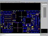 Snapper255 bottom components in Cadence Allegro |

Bluewater Systems also developed a complex vehicle tracking system (project name Dory) which integrates a Snapper CL15, GPS, GPRS, Bluetooth, 1GB of storage and other features. These are two separate boards stacked together and each PCB just measures 90x50mm approximately.
Dory


Rig200 Component Placement
The Rig200 board form-factor was designed around the shape of a standard 5.25” CD-ROM bay. It measures just 140x199mm but packed with features such as WiFi, Bluetooth, GSM / GPRS, GPS, Compact Flash, Batteries, LCD controller, SD card, USB, Ethernet (with PoE), NAND storage to name a few. It also supports all Snapper modules including the SO-DIMM version.
Rig 200