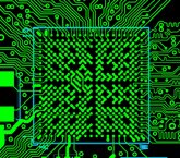
Quad-Flat No-Lead (QFN) packages are very popular and widely used nowadays in the semiconductor industry. Its primary advantages compared to leaded packages (SOICS, SSOPs, QFPs, etc.) are its small size and greatly enhanced thermal capability, which transforms into more power handling. Let's repeat it, more power in a small size, which fits into the present script of today's electronic gadgets and products: keep it small. At Bluewater Systems, QFNs are always present in every moderate to complex board design. There are a lot of advantages with this package compared to leaded packages, but it is not the advantages that cause this blog to be written. It is something about the way they are presented in the data sheet and the way that they are typically called out for a given number of pins (e.g. QFN32 or 32-pin QFN). Normally, a device's data sheet contains the "features" list which includes the device's package in the very first page, such as, "6x6 32-leadless QFN or 4x4 16-leadless QFN". But here's the catch, QFN doesn't always imply equal number of pads on all four sides making it square in form. It can also be rectangular, which means two sides have a lesser number of pads than the other two. QFN16 could mean 4x4 pads on all sides (image on the left) or 2x6 pads (6 pads on the longer side and 2 on the shorter side, image on the right) and so on. 
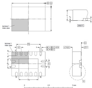
 In PCB design, it is always a standard procedure to check the mechanical dimensions of the package to map a correct footprint, even with conventional lead packages. Usually, a package's mechanical details are put on the last few pages in a data sheet. Worse, some data sheets don't even provide the mechanical details of the package (though this is rare for devices in a QFN package) based on experience. It is sometimes hidden in the manufacturers website. However, in large complex boards, there may be multiple devices in QFN packages with the same number of pads but different pad configurations (square or rectangular in form) which could be prone to human error by interchanging footprints at the pre-layout stage. So, extra car must be taken when dealing with QFNs. At Bluewater Systems, as part of its evolving quality procedures, a special footprint naming convention for QFNs has been adopted. It must include a QFNs pitch, pad configuration (number of pads in two adjacent sides) and package size. It's quite a lengthy naming than the conventional footprint naming before QFNs were popular, but it is effective in eliminating errors.

Quad-Flat No-Lead (QFN) Packages: What About Them?Posted in Uncategorized on May 20, 2009 by Janus Patalinjug Xnets & PCB Layout tool documentationPosted in Uncategorized on November 11, 2008 by Janus Patalinjug While working on DDR memory routing on our Snapper-DV board, which is now using a Texas Instruments (TI) OMAP3530 applications processor, all DDR memory bus lines, including control signals, are terminated with series resistors in between the processor going to the two balance-T DDR ICs. As with all routing that involves DDR, extensive length matching is normally applied to these memory traces (which are further classified into classes per their function). Normally, Cadence Allegro Performance tool via Constraint Manager can handle length matching of traces point-to-point (net) very well. But with series termination resistors in between, it adds complication because these resistors have to be inerpreted as part of the net connecting the processor to the DDR ICs (see figure below) and thus have to be included in the length matching. When the path of a net traverses a discrete device (resistor, inductor or capacitor), each net segment is represented by an individual net entity (net1, net2) and this whole length is called "Extended Nets" or Xnets. CPU ------------ series term resistors ------------ DDR ICs net1 net2 |-------- Extended Nets (Xnets) ---------| Cadence handles Xnets very well and it's very well documented using their high-end schematic/PCB layout and simulation tools, which are very costly. Xnets have to be created so that Constraint Manager can interpret this as a whole trace/track length for matching. These can only be created by attaching a "signal model" on the discrete device (resistor in our case) and this is a very easy step with Cadence high-end tools front-to-back flow as it is well documented. But with a basic ConceptHDL and Allegro Performance tools, it took some fiddling around to achieve the task. Though the Allegro Performance datasheet shows that Xnets are supported, getting the Constraint Manager to recognize the Xnets was not easy. Assigning a "signal_model" property using the "Edit>Properties" menu was easy, but it didn't create the Xnet that was expected. There are no explicit instructions on how to do this on this medium-flavored tool. The trick was to go through "Setup Advisor" until "SI Model Assignments" and assign the "signal_model" property to the resistors. This procedure worked, Xnets were created, Constraint Manager did recognize these and length matching can now be handled optimally and with ease. In summary, and from experience with using schematic/PCB software tools not just from Cadence, it just doesn't end going thorugh the documentation of using the tool. There's a lot more to it when using and applying the tools in real life work. Bluewater, PCB Design & Fine-Pitch BGAsPosted in Hardware design on September 26, 2008 by Janus Patalinjug PCB design at Bluewater is most of the time an exciting challenge, especially when it comes with system modules. Just like with any other modern digital gadgets nowadays, they have to be small in size and thus, space (or real estate as another term used by PCB designers) on a PCB is always a premium. Along with this direction, the chain must adapt to it, small fine-pitch and high density components are mostly used, PCB vendors have to update their capability, as well as PCB assembly houses. And of course, cost will always be involved when going to miniature, complicated technology. Otherwise, these modern tiny gadgets will never exist. Speaking of fine-pitch high density components, things like 0.5 to 0.65mm pitch BGA packages should usually surface as a common option along with fine-pitch packages such as QFN, DFN, etc. The thing with fine-pitch BGAs, especially full-matrix ones, is that they are usually more difficult to fan-out (so that you can route to the rest of the circuitry on the PCB) compared to conventional0.8 to 1mm pitch BGAs. High-tech PCB technologies such as Two year ago, we developed a module (37mm x 26mm) with Intel's PXA272 microprocessor (0.65mm-pitch, 336 pins, full matrix BGA) on it for our customer (in military defence). With cost in mind and by coordinating with our PCB vendor, we were able to avoid the costly high-tech HDI or blind/buried microvias, or via-in-pad by using 5-mil via through-hole drill/15-mil via pad and 3-mil spacing between vias to any other entities but with limited aspect ratio. Although this approach may still not fall under (still slightly expensive) the conventional PCB technologies and is dependent of our PCB vendor, at least it's not a full blown HDI or any other costly cutting edge PCB technology and it's good to know that there are less costly options like this, especially when just producing prototype quantities. In our Snapper 270 SOM, we also have buffers having 0.65mm pitch but not full-matrix ones and we were able to use full conventional PCB technology by carefully assigning signals on the buffer side to eliminate vias in fanning out the BGA and optimised routing. Most recently, we are currently developing our Snapper-DV board, which is using Texas Instrument's Da Vinci processor TMS320DM355, a full-matrix, 377 pin, 0.65mm pitch BGA and again, the same above mentioned strategy were used to check cost and this time around, with an improved aspect ratio, thanks to our PCB vendor. |
 In the near future, HDI and the like may be the only way to go but hopefully, the cost tagged along with using these cutting-edge technologies will trick down (fingers crossed).

