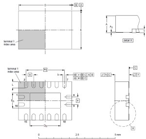
Quad-Flat No-Lead (QFN) packages are very popular and widely used nowadays in the semiconductor industry. Its primary advantages compared to leaded packages (SOICS, SSOPs, QFPs, etc.) are its small size and greatly enhanced thermal capability, which transforms into more power handling. Let's repeat it, more power in a small size, which fits into the present script of today's electronic gadgets and products: keep it small. At Bluewater Systems, QFNs are always present in every moderate to complex board design. There are a lot of advantages with this package compared to leaded packages, but it is not the advantages that cause this blog to be written. It is something about the way they are presented in the data sheet and the way that they are typically called out for a given number of pins (e.g. QFN32 or 32-pin QFN). Normally, a device's data sheet contains the "features" list which includes the device's package in the very first page, such as, "6x6 32-leadless QFN or 4x4 16-leadless QFN". But here's the catch, QFN doesn't always imply equal number of pads on all four sides making it square in form. It can also be rectangular, which means two sides have a lesser number of pads than the other two. QFN16 could mean 4x4 pads on all sides (image on the left) or 2x6 pads (6 pads on the longer side and 2 on the shorter side, image on the right) and so on. 
 In PCB design, it is always a standard procedure to check the mechanical dimensions of the package to map a correct footprint, even with conventional lead packages. Usually, a package's mechanical details are put on the last few pages in a data sheet. Worse, some data sheets don't even provide the mechanical details of the package (though this is rare for devices in a QFN package) based on experience. It is sometimes hidden in the manufacturers website. However, in large complex boards, there may be multiple devices in QFN packages with the same number of pads but different pad configurations (square or rectangular in form) which could be prone to human error by interchanging footprints at the pre-layout stage. So, extra car must be taken when dealing with QFNs. At Bluewater Systems, as part of its evolving quality procedures, a special footprint naming convention for QFNs has been adopted. It must include a QFNs pitch, pad configuration (number of pads in two adjacent sides) and package size. It's quite a lengthy naming than the conventional footprint naming before QFNs were popular, but it is effective in eliminating errors.

- Error
Quad-Flat No-Lead (QFN) Packages: What About Them?Posted in Uncategorized on May 20, 2009 by Janus Patalinjug Interesting Survey Results on MSD StandardsPosted in Industry News on May 18, 2009 While reading a series of articles posted on www.pcb007.com relating to IPC and Jedec Standards, I was surprised to see the results of a survey they carried out with regards to the new and updated MSD (moisture sensitive devices) standards release late last year. These standards are J-Std-020, J-Std-033 and the new J-Std-075. While two of these are updated revisions of the old standards they still do hold a lot of new valuable information, especially when it comes to higher reflow and wave soldering temperatures. However, the J-Std-075 is new and one can expect this to change and be updated as the industry evaluates this further. Or perhaps not, as the results of the survey showed that these standards are currently not really being conformed to. Baking parts before use can be a costly and time consuming exercise and one that may be seen to have to real benefit. However, when you consider that not putting simple processes in place to prevent damage can decrease yields, not to mention wasting what could be valuable components, the cost of not doing so can soon add up. What this shows me is that you can't just give an assembly house a bunch of parts, some PCB's and expect them to deliver functional and reliable products with high yields. (Although this is exactly what everyone would like to see happen.) Any electronic design house needs to know what standards their suppliers adhere to and what consequences may occur if their chosen production facility does not apply these standards. This does require a design house to keep up to date with manufacturing standards. This is especially true when you consider MSD damage to devices. The units may pass any production testing bu fail later in the field. This puts the failure back into the hands of the design house who then needs to deal with the RMA returns and upset customers. Another important question not to be overlooked is how widely known are these standards? Do IPC and Jedec need to do more to promote the use of these standards within the industry? Based on the results of the survey, it seems more in the court of the customer, i.e. any design house. Once a customer starts to request compliance to the standards, component manufacturers/suppliers and contract manufacturers will put the required processes in place. |


